“Nanometer-scale” surface roughness may seem rare and specialized. But, in fact, many components and common products require nanometer-scale, or sub-nanometer-scale, average roughness (Sa) in order to function properly.
The ability to properly measure and control fine roughness such as this requires accurate metrology and an understanding of the relationship between the texture and the component’s intended function.
Automotive finishes
To create a long-lasting, good-looking automotive finish, a manufacturer must control each film’s thickness to tight tolerances, on panels with complex curvature and many small features. A painted panel will ultimately have a protective top coat with nanometer-scale surface roughness that allows the light to easily penetrate and reflect from the decorative base coat pigments.
Challenges abound when measuring this thin, transparent layer. With careful setup we can measure the top surface of the topcoat which is typically ~10 µm thick. However, if the paint includes metal flake, we may have to contend with spike reflections as well.
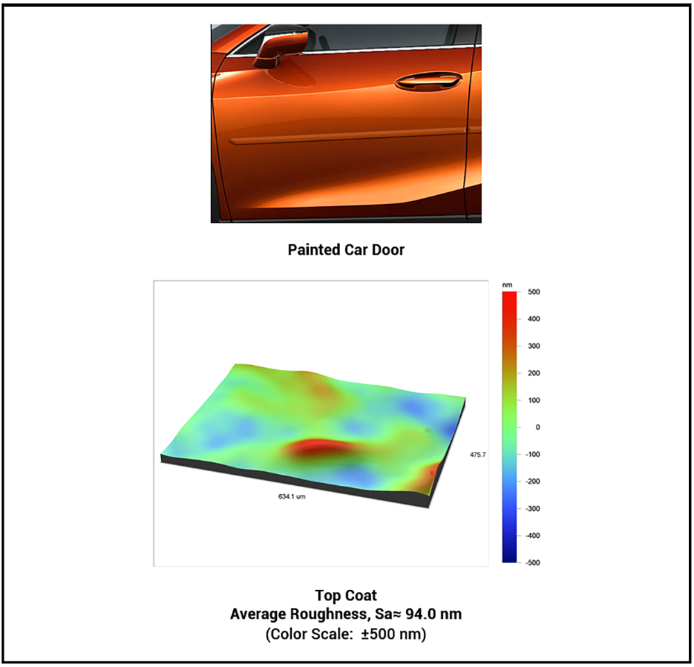
There is some great work being done on the topic, including this paper by Christopher M. Seubert.
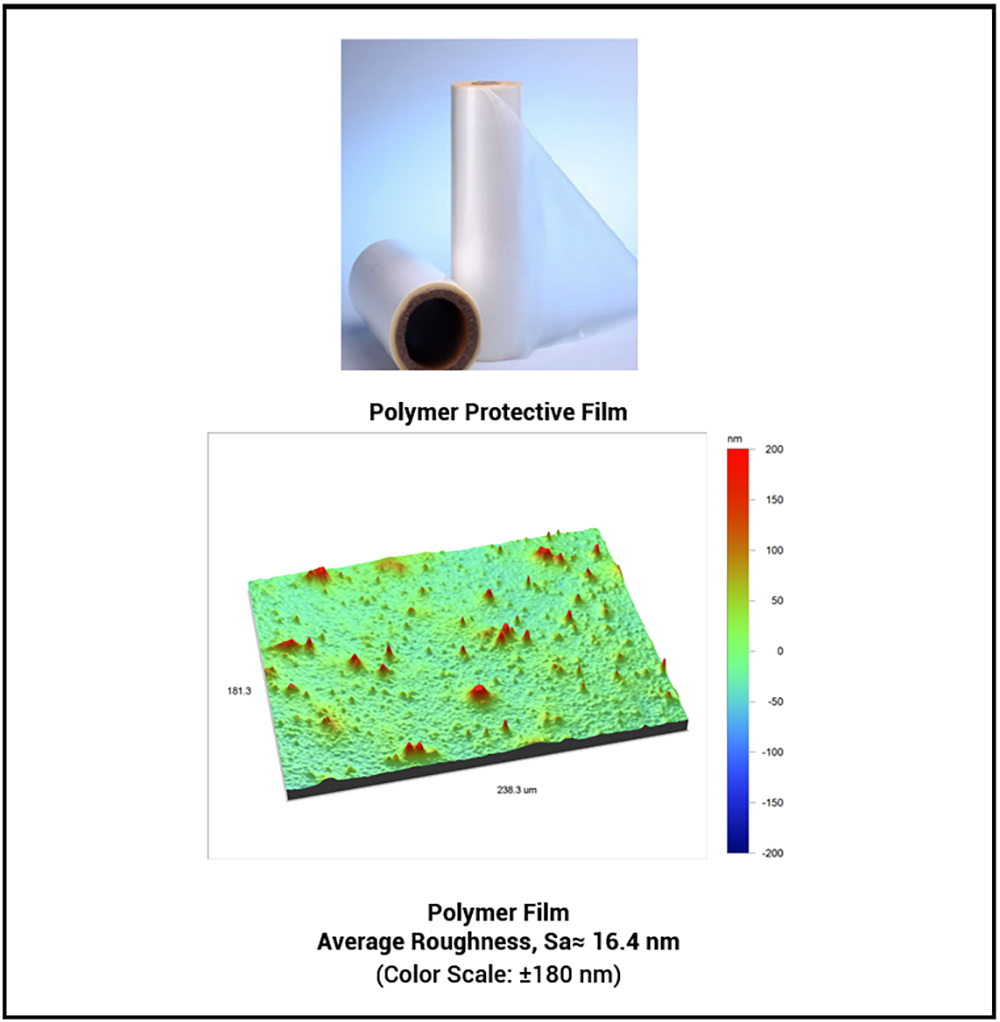
Plastic packaging
Packaging may seem like a low-tech application—yet, the engineering that goes into protective films can be as involved, and ingenious, as any tech product.
Take, for example, plastic films used to protect critical surfaces. The roughness of these films is held to nanometers in Sa. At the same, time, regular asperities of carefully controlled height and diameter ensure that the film can be easily removed from the protected device.
Both the field roughness and the asperities are critical to the function. Measuring both on (typically) clear films requires careful measurement, typically using optical 3D methods. A thorough understanding of filtering is also required to separate the asperities from the roughness.
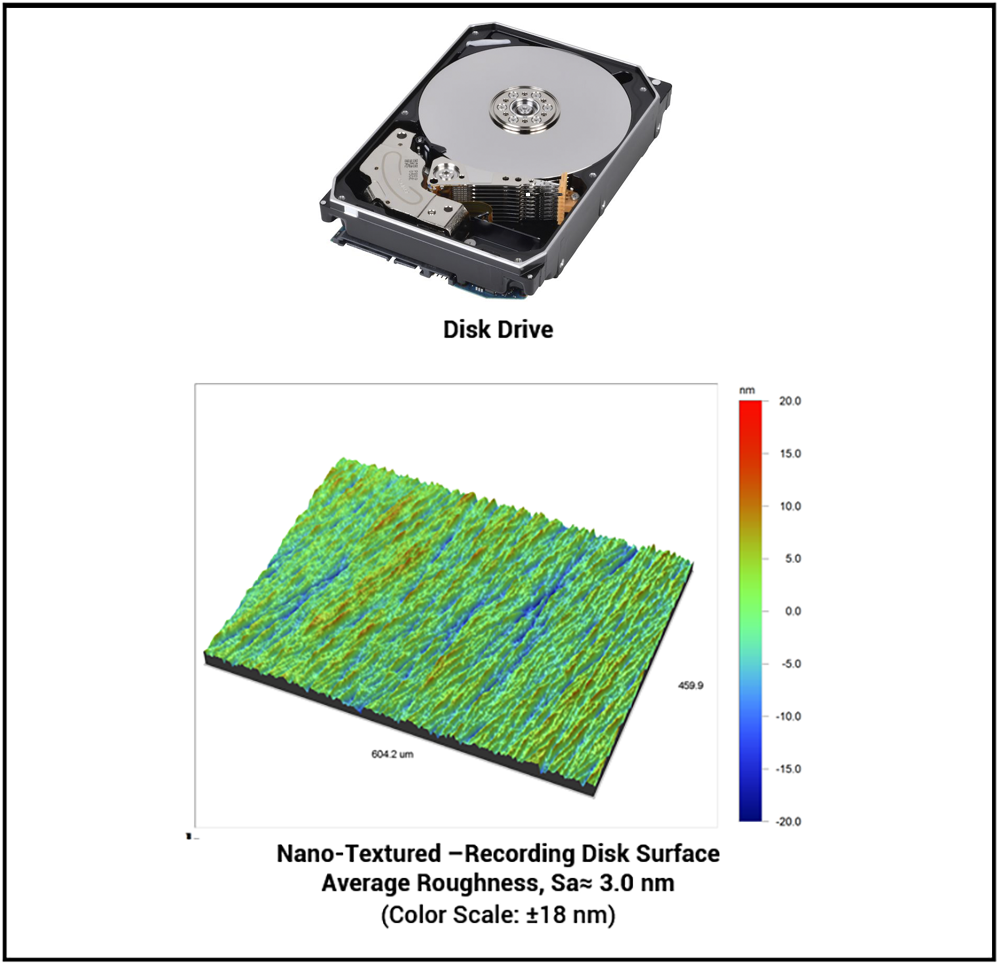
Disk drive
It’s been said that a disk drive read head moving over a data storage disk is comparable to a 747 airplane flying less than 0.05 cm above the ground, at speed, while never making contact.
To accomplish this amazing feat, disk drive platters are manufactured with highly engineered, nanometer-scale surface texture that must: a) enable the read head to fly incredibly close to the surface, and b) minimize stiction when the recording head is parked on a stopped disk, so that it can quickly resume its motion.
Controlling the shape and density of these intentional asperities is typically accomplished through optical profilometry. The combination of fast measurement times, non-contact measurement, high resolution and repeatability means that these instruments can measure in-line, at production speed.
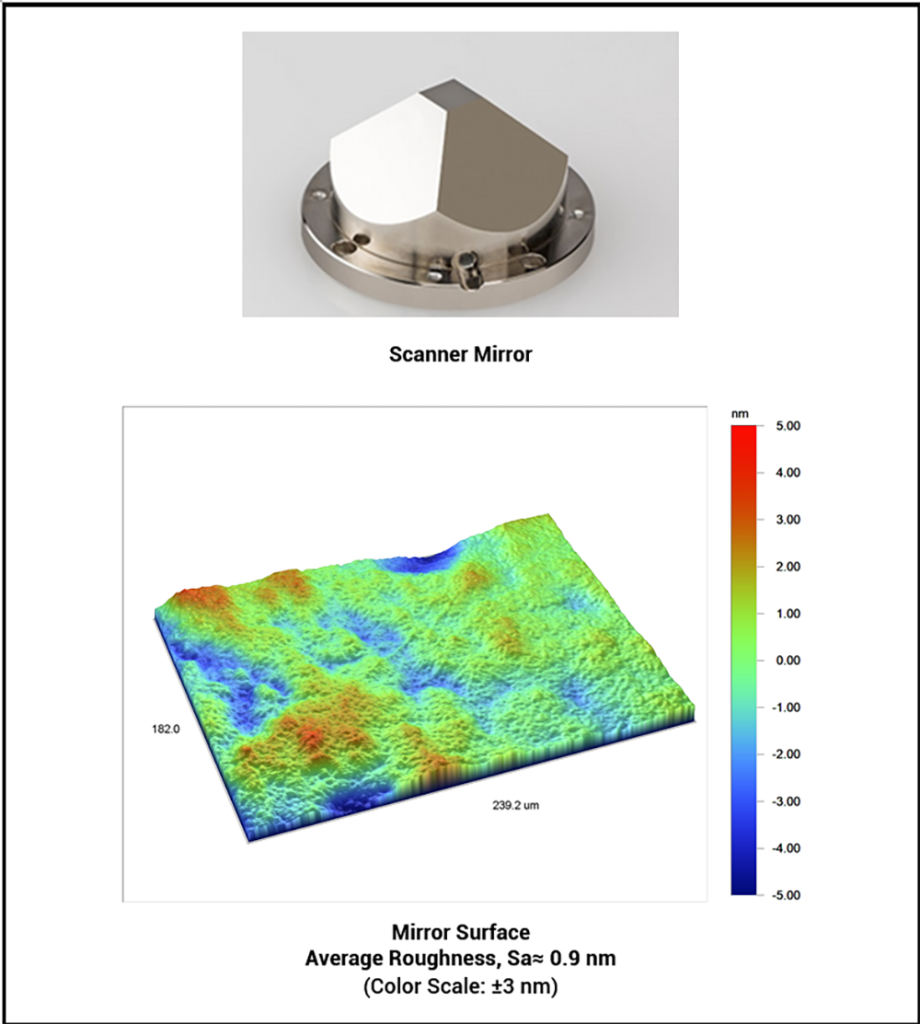
Scanner mirror
A typical mirror used in an optical device (a supermarket scanner, for example), may require sub-nanometer roughness, Sa, to minimize light scatter and provide clear imaging.
The image below shows a scanner mirror and surface data acquired with a 3D optical profiler. This extremely smooth surface requires the ultimate in measurement techniques known as Phase Shifting Interferometry, which offers height resolutions measured in Angstroms (0.1 nm = 1 Angstrom).